Projet:Contrôler très simplement un SI5351 avec un Attiny85 programmé via l’ide Arduino 1.8.7.
Attention testé jusqu’à version micronucleus 1.06 (1.6).
1.Matériel.
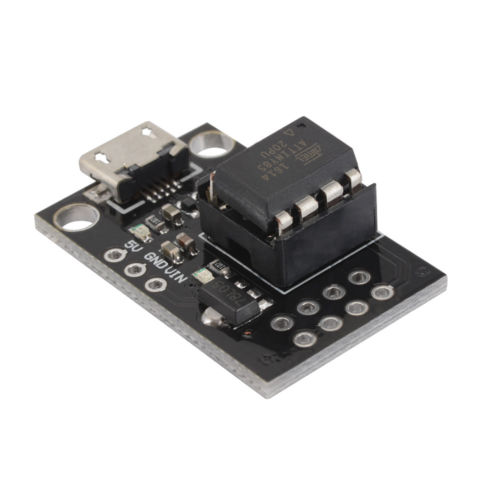
Commandé sur ebay: ATtiny85-20PU IC DIP-8 MCU Micro USB Development Programmer Board Pins TE769
2.Installation de l’IDE et des paquets.
D’après cette source: https://digistump.com/wiki/digispark/tutorials/connecting
Une fois l’ide arduino installé sur votre machine:
-Aller dans Fichier>Préférences
-Dans « url de gestionnaire de cartes supplémentaires »
-Ajouter « https://digistump.com/wiki/digispark/tutorials/connecting »
-Terminer en cliquant sur « Ok »
-Aller dans Outils>Types de cartes>Gestionnaire de cartes et chercher « Digistump » selectionner « Digistump AVR Boards » puis cliquer sur « Installer »
-Une fois installé, aller dans Outils>Types de cartes et sélectionner « Digispark (Default – 16,5mhz) »
Voila, vous êtes prêt pour vos premiers tests.
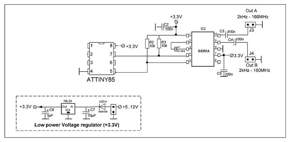
3.Connexion au SI5351
4.Le code
|
1 2 3 4 5 6 7 8 9 10 11 12 13 14 15 16 17 18 19 20 21 22 23 24 25 26 27 28 29 30 31 32 33 34 35 36 37 38 39 40 41 42 43 44 45 46 47 48 49 50 51 52 53 54 55 56 57 58 59 60 61 62 63 64 65 66 67 68 69 70 71 72 73 74 75 76 77 78 79 80 81 82 83 84 85 86 87 88 89 90 91 92 93 94 95 96 97 98 99 100 101 102 103 104 105 106 107 108 109 110 111 112 113 114 115 116 117 118 119 120 121 122 123 124 125 126 127 128 129 130 131 132 133 134 135 136 137 138 139 140 141 142 143 144 145 146 147 148 149 150 151 152 153 154 155 156 157 158 159 160 161 162 163 164 165 166 167 168 169 170 171 172 173 174 175 176 177 178 179 180 181 182 183 184 185 186 187 188 189 190 191 192 193 194 195 196 197 198 199 200 201 |
#include <avr/pgmspace.h> #include <Wire.h> #define SI5351_i2c_bus_addr 0x60 #define SI5351_PLLA 0 #define SI5351_PLLB 1 void si5351_init() { Wire.beginTransmission(SI5351_i2c_bus_addr); uint8_t reg_val; reg_val = Wire.endTransmission(); if (reg_val == 0) { uint8_t status_reg = 0; do { status_reg = si5351_read(0); } while (status_reg >> 7 == 1); /* Disable all outputs setting CLKx_DIS high */ si5351_write(3, 0xFF); // Initialize the CLK outputs according to flowchart in datasheet // First, turn them off si5351_write(16, 0x80); si5351_write(17, 0x80); si5351_write(18, 0x80); // Turn the clocks back on... si5351_write(16, 0x0c); si5351_write(17, 0x0c); si5351_write(18, 0x0c); /* Set the load capacitance for the XTAL */ si5351_write(183, (0 << 6)); } } void si5351_setupPLL(uint8_t mult, uint32_t num = 0, uint32_t denom = 1, bool pll = 0)//pll 1 = pllB default pllA { uint32_t P1; /* PLL config register P1 */ uint32_t P2; /* PLL config register P2 */ uint32_t P3; /* PLL config register P3 */ P1 = (uint32_t)(128 * mult + floor(128 * ((float)num / (float)denom)) - 512); P2 = (uint32_t)(128 * num - denom * floor(128 * ((float)num / (float)denom))); P3 = denom; uint8_t baseaddr = (pll == 0 ? 26 : 34); /* The datasheet is a nightmare of typos and inconsistencies here! */ si5351_write( baseaddr, (P3 & 0x0000FF00) >> 8); si5351_write( baseaddr + 1, (P3 & 0x000000FF)); si5351_write( baseaddr + 2, (P1 & 0x00030000) >> 16); si5351_write( baseaddr + 3, (P1 & 0x0000FF00) >> 8); si5351_write( baseaddr + 4, (P1 & 0x000000FF)); si5351_write( baseaddr + 5, ((P3 & 0x000F0000) >> 12) | ((P2 & 0x000F0000) >> 16) ); si5351_write( baseaddr + 6, (P2 & 0x0000FF00) >> 8); si5351_write( baseaddr + 7, (P2 & 0x000000FF)); /* Reset both PLLs */ si5351_write(177, (1 << 7) | (1 << 5) ); } void si5351_setupMultisynth(uint8_t output, uint32_t div, uint32_t num = 0, uint32_t denom = 1, bool pllSource = 0) //pllsource 1 = pllB default pllA { uint32_t P1; /* Multisynth config register P1 */ uint32_t P2; /* Multisynth config register P2 */ uint32_t P3; /* Multisynth config register P3 */ if (num == 0) { /* Integer mode */ P1 = 128 * div - 512; P2 = num; P3 = denom; } else { /* Fractional mode */ P1 = (uint32_t)(128 * div + floor(128 * ((float)num / (float)denom)) - 512); P2 = (uint32_t)(128 * num - denom * floor(128 * ((float)num / (float)denom))); P3 = denom; } /* Get the appropriate starting point for the PLL registers */ uint8_t baseaddr = 0; switch (output) { case 0: baseaddr = 42; break; case 1: baseaddr = 50; break; case 2: baseaddr = 58; break; } /* Set the MSx config registers */ si5351_write( baseaddr, (P3 & 0x0000FF00) >> 8); si5351_write( baseaddr + 1, (P3 & 0x000000FF)); si5351_write( baseaddr + 2, (P1 & 0x00030000) >> 16); /* ToDo: Add DIVBY4 (>150MHz) and R0 support (<500kHz) later */ si5351_write( baseaddr + 3, (P1 & 0x0000FF00) >> 8); si5351_write( baseaddr + 4, (P1 & 0x000000FF)); si5351_write( baseaddr + 5, ((P3 & 0x000F0000) >> 12) | ((P2 & 0x000F0000) >> 16) ); si5351_write( baseaddr + 6, (P2 & 0x0000FF00) >> 8); si5351_write( baseaddr + 7, (P2 & 0x000000FF)); /* Configure the clk control and enable the output */ uint8_t clkControlReg = 0x0F; /* 8mA drive strength, MS0 as CLK0 source, Clock not inverted, powered up */ if (pllSource) clkControlReg |= (1 << 5); if (num == 0) clkControlReg |= (1 << 6); /* Integer mode */ switch (output) { case 0: si5351_write(16, clkControlReg); break; case 1: si5351_write(17, clkControlReg); break; case 2: si5351_write(18, clkControlReg); break; } } uint8_t si5351_enable() { si5351_write(3,0x00); } uint8_t si5351_write(uint8_t addr, uint8_t data) { Wire.beginTransmission(SI5351_i2c_bus_addr); Wire.write(addr); Wire.write(data & 0xFF); return Wire.endTransmission(); } uint8_t si5351_read(uint8_t addr) { uint8_t reg_val = 0; Wire.beginTransmission(SI5351_i2c_bus_addr); Wire.write(addr); Wire.endTransmission(); Wire.requestFrom(SI5351_i2c_bus_addr, (uint8_t)1); while (Wire.available()) { reg_val = Wire.read(); } return reg_val; } void setup() { Wire.begin(); si5351_init(); delay(100); si5351_setupPLL(34, 82, 125, SI5351_PLLA); delay(100); si5351_setupPLL(32, 16, 125, SI5351_PLLB); delay(100); si5351_setupMultisynth(0, 28, 68, 141, SI5351_PLLB); delay(100); si5351_setupMultisynth(1, 16, 0, 1, SI5351_PLLB); delay(100); si5351_setupMultisynth(2, 6, 0, 1, SI5351_PLLA); delay(100); si5351_enable(); delay(100); } void loop() { } |
5.Calculer ces PLL
Source: https://learn.adafruit.com/adafruit-si5351-clock-generator-breakout/wiring-and-test
Télécharger et install le ClockBuilder: http://www.adafruit.com/downloads/ClockBuilderDesktopSwInstallSi5351.zip
Lancer le, séléctionner « SI55351A on Timming TollStick », « Ok », Entrer la ou les fréquences :
-du chrystall soit 25 ou 27 mhz
-Cocher une, deux ou trois premières enable channel
-entrer la ou les fréquences de sortie souhaitées
Puis cliquez sur « Create Frequency plan » et enfin sur « View Plan Détails » juste en dessous.
J’obtiens:
|
1 2 3 4 5 6 7 8 9 10 11 12 13 14 15 16 17 18 19 20 21 22 23 24 25 26 27 28 29 30 31 32 33 34 35 36 37 38 39 40 41 42 43 44 45 46 47 48 |
PLL A Input Frequency (MHz) = 25,000000000 VCO Frequency (MHz) = 866,400000000 Feedback Divider = 34 82/125 SSC disabled PLL B Input Frequency (MHz) = 25,000000000 VCO Frequency (MHz) = 803,200000000 Feedback Divider = 32 16/125 Output Clocks Channel 0 Output Frequency (MHz) = 28,200000000 Multisynth Output Frequency (MHz) = 28,200000000 Multisynth Divider = 28 68/141 R Divider = 1 PLL source = PLLB Initial phase offset (ns) = 0,000 Powered down = No Inverted = No Drive Strength = b11 Disable State = Low Clock Source = b11 Channel 1 Output Frequency (MHz) = 50,200000000 Multisynth Output Frequency (MHz) = 50,200000000 Multisynth Divider = 16 R Divider = 1 PLL source = PLLB Initial phase offset (ns) = 0,000 Powered down = No Inverted = No Drive Strength = b11 Disable State = Low Clock Source = b11 Channel 2 Output Frequency (MHz) = 144,400000000 Multisynth Output Frequency (MHz) = 144,400000000 Multisynth Divider = 6 R Divider = 1 PLL source = PLLA Initial phase offset (ns) = 0,000 Powered down = No Inverted = No Drive Strength = b11 Disable State = Low Clock Source = b11 |
Dans la partie setup de mon code j’aurai:
|
1 2 3 |
si5351_setupPLL(34, 82, 125, SI5351_PLLA); Soit 25MHz * (m + n/d) = 25MHz * (34 + 82/125) = 866,400000000Mhz pour PLLA |
|
1 2 3 |
si5351_setupPLL(32, 16, 125, SI5351_PLLB); Soit 25MHz * (m + n/d) = 25MHz * (32 + 16/125) = 803,200000000Mhz pour PLLB |
Puis on redivise vers les sorties
|
1 2 3 |
si5351_setupMultisynth(0, 28, 68, 141, SI5351_PLLB); =>803,2 / (28 + 68/141) = 28,2mhz |
|
1 2 3 |
delay(100); si5351_setupMultisynth(1, 16, 0, 1, SI5351_PLLB); =>803,2 / (16 + 0/1) = 50,2mhz |
|
1 2 3 |
delay(100); si5351_setupMultisynth(2, 6, 0, 1, SI5351_PLLA); =>866,4 / (6 + 0/1) = 144,4mhz |
Enfin, on active les sorties:
|
1 |
si5351_enable(); |